|
VG TECHNOLOGIES CO., LIMITED
|
VGT ML PCB 0002
| Payment Terms: | T/T,L/C,D/A,D/P,WU |
| Place of Origin: | Guangdong, China (Mainland) |
|
|
|
| Add to My Favorites | |
| HiSupplier Escrow |
Product Detail
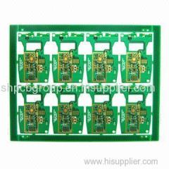
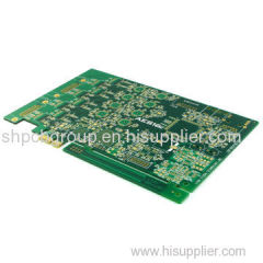
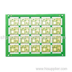
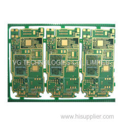
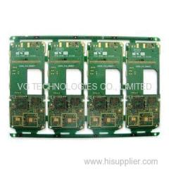
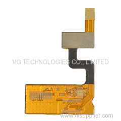
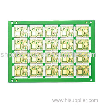
china pcb manufacturer, multilayer, VGT
Specifications:
Layers: 1 to 48
Board finished thickness: 0.21 to 7.0mm
Materials: FR-4, CEM-1, CEM-3, high TG, FR4 halogen free,Rogers
Maximum finished board size: 23 x 25mm (580 x 900mm)
Minimum drilled hole size: 3 mils (0.075mm)
Minimum line width: 3 mils (0.075mm)
Minimum line spacing: 3 mils (0.075mm)
Size: 243.4 x 244.43mm
Surface finishing/treatment: HASL/HASL lead-free, HAL, chemicaltin, chemical gold,
immersion silver/gold, OSP, gold plating
Copper thickness: 0.5 to 7.0oz
Solder mask colors: green, yellow, black, white, red, blue
Copper thickness in hole: >25.0µm (>1 mil)
Packing:
Inner packing: vacuum packing/plastic bag
Outer packing: standard carton packing
Shape tolerance: ±0.13
Hole tolerance:
PTH: ±0.076
NPTH: ±0.05
With UL, SGS and RoHS marks
Special requirements: buried and blind via + controlledimpedance + BGA
Profiling: punching, routing, V-cut, beveling
Testing procedure:
Visual inspection
Flying probe
Impedance control
Solder-ability detection
Digital metallographic microscope
AOI (automated optical inspection)
circuito stampato,circuito impreso,kretskort,circuito impresso,circuit imprimat,Plošný spoj,printplaat,circuit imprimé,печатная плата,Leiterplatte,printplade,Płytki PCB produkcja,Obwody drukowane,PCB valmistamise,PCB Monaraithe,PCB fabbrica,PCB mhonarcha,circuit imprimé usine,circuito stampato fabbrica,kretskort fabrik,Leiterplattefabrik,circuit board
multilayered circuit board,PCB fabrication,HDI PCB,PCB layout,quick turn,one-stop service,aluminum based pcb,flexible circuit board,FPC,BGA board,impendance control,double-sided pcb
Services:
No MOQ
Provide OEM services
Multilayer PCB sample: 6-10 days, mass production: within 15 days
Double-sided PCB sample: 3-5 days, mass production: within10 days
Shipping methods: DHL, UPS, FedEx, TNT forwarder
Didn't find what you're looking for?
Post Buying Lead or contact
HiSupplier Customer Service Center
for help!
Related Search
Find more related products in following catalogs on Hisupplier.com
Company Info
VG TECHNOLOGIES CO., LIMITED [China (Mainland)]
Business Type:Manufacturer
City: Shenzhen
Province/State: Guangdong
Country/Region: China (Mainland)